 |
|||
|
|
|||
|
|
|||
| ||||||||||
|
|
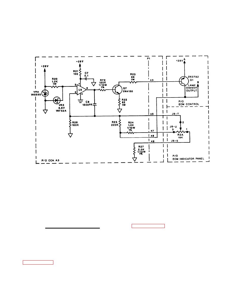 TM 32-5865-218-24&P
Countermeasures Control Lamp Control Circuits
Simplified Schematic Diagram
external system equipment at connector J4. Contacts 2 and 3 close to
provide ground to external system equipment at connector pin J8-H.
When the FM antenna control input goes high, the switch restores, and
contacts 2 and 3 open.
Front
Refer to figure FO-2, sheet 2.
c. Voltage Regulator A1.
panel circuit breaker CB1 protects the +28 V dc unfiltered mission
power input to voltage regulator A1. When DC POWER circuit breaker
CB1 is set to the on (in) position, the +28 V dc input at connector
pin J3-X passes through connector pin A1P1-1 to voltage regulator
The lamp adjust inputs from external system equipment
assembly A1.
at connector pins J8-V and J8-X pass through connector pins A1P1-4
and A1P1-5, respectively, to control voltage regulators VR1 and VR2
through connector pins A1P1-2, A1P1-3, J8-Y, and J8-a to external
system equipment.
|
|
Privacy Statement - Press Release - Copyright Information. - Contact Us |
