 |
|||
|
|
|||
|
Page Title:
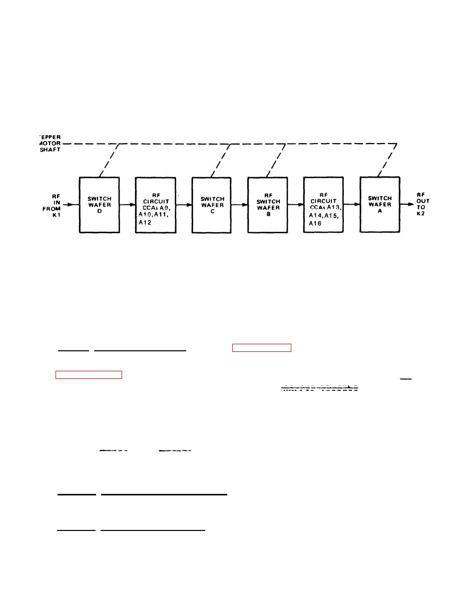
Figure 3-5. RF Switch Assembly S2 Block Diagram |
|
||
| ||||||||||
|
|
 TM 32-5865-216-24&P
RF Switch Assembly S2 Block Diagram
The decoder CCA status
circuit consists of filters CR1, CR2, R5, and C16; line receiver
U18B; AND gate U4C; NAND gate U7; and line driver U19. As shown in
Line receiver U18B converts the DF input into a DF
NAND gate U7-5.
The READY and INVALID ADDRESS inputs from
signal to NAND gate U7-3.
control logic CCA A3 are applied to NAND gate U7-2 and NAND gate
AND gate U4C receives the BUF 1-MHz output of
U7-6, respectively.
multivibrator U14B and the TEMP DET input from switch S3 in RF switch
The U4C output is inverted and passes to NAND gate U7-12
assembly S2.
The inverted U4C output also passes to
as the CLOCK READY signal.
In addition, NAND gate U7 receives
extender CCA A5 as the TOL signal.
PARITY, RESET, and MANCON 2 signals from flip-flop U6B, multivibrator
The U7-8 output through line
UL4A, and flip-flop U5B, respectively.
driver U19A indicates status conditions as follows:
The digital output signal is a
3-6.1.1 Not Ready for Commands.
logic low when the tunable coupler is performing any operation that
inhibits receipt of a command word.
The digital output signal is a logic
3-6.1.2 Ready for Commands.
high when all of the following conditions are met:
|
|
Privacy Statement - Press Release - Copyright Information. - Contact Us |
